Prof. Junseop Shim (Electronics) Develops Semiconductor Technology Without Photolithography
- admin
- 2024-11-04
- 85
· Professor Junseop Shim (Department of Electronics Convergence Engineering) Develops Semiconductor Process Technology Without Photolithography
- Developed technology for creating fine patterns for
biosensor applications without expensive photolithography process -
- Paper published in Biosensors and Bioelectronics
(JCR Q1 Ranking, Impact Factor: 10.7) -
Professor
Junseop Shim's research team in the Department of Electronics Convergence
Engineering at Kwangwoon University has developed a technology for creating
fine metal patterns without the costly photolithography process, successfully
applying it to biosensors that can sensitively measure dementia marker
concentrations in blood. Professor Junseop Shim's research team used the newly
developed technology to create high-sensitivity biosensors with fine metal
patterns in a disposable, single-use format.
The research results were
published in Biosensors and Bioelectronics, a leading SCI journal in the field
of biosensors.
(Reference: https://www.sciencedirect.com/science/article/abs/pii/S0956566323007339)

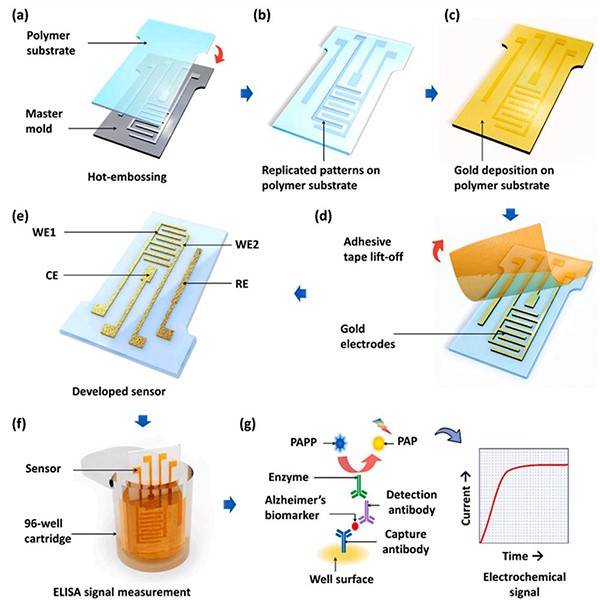
Creating fine metal patterns requires a multi-step semiconductor process known as photolithography. The photolithography process requires expensive equipment, making production costly, and it is not environmentally friendly due to the use of photoresists and developers. However, to measure trace amounts of Alzheimer’s biomarkers in the blood, a highly sensitive biosensor is necessary, making the production of fine metal patterns crucial. However, biosensors developed in this way are expensive to manufacture, which makes disease testing with biosensors expensive.
To address this issue,
Professor Shim’s team developed a method that uses molds with fine patterns to
repeatedly stamp fine patterns onto plastic substrates. The plastic substrate
is then coated with a thin metal film, and tape is applied so that the metal
film comes into contact with the tape. Since the fine patterns are recessed,
they do not touch the tape, and when the tape is peeled off, the metal remains
only in the fine-patterned areas. This process allowed the team to create fine
metal patterns on plastic substrates, which were then applied to dementia
diagnostic biosensors, enabling the detection of two dementia markers at low
concentrations of 3.9 pg/ml and 7.81 pg/ml, respectively.
Professor Shim stated,
“To create a high-sensitivity biosensor that can measure dementia markers and
be used as a disposable product, we developed a semiconductor fine-patterning
technology that does not require photolithography. This technology can be applied
not only to biosensors but also to the development of various electronic
devices, including semiconductors, displays, and sensors that require fine
metal patterns.”
This
research was supported by the Korea Medical Device Development Fund, Korea
Dementia Research Center, and Kwangwoon University’s internal research funding.
The research results were published in
Biosensors and Bioelectronics, a prestigious journal published by Elsevier (JCR
Q1 ranking, Impact Factor: 10.7).