Professor Ha Tae-Jun's Research Team Identifies Charge Transfer Mechanism
- admin
- 2024-12-17
- 1233
· Professor Ha Tae-Jun's Research Team (Department of Electronic Materials Engineering) Identifies Charge Transfer Mechanism in High-Mobility Indium-Gallium-Zinc Oxide Thin-Film Transistors Based on Atomic Layer Deposition
Views 134 | Created
2024.12.09 | Modified 2024.12.09 | Public Relations Team
·
Professor
Ha Tae-Jun's Research Team (Department of Electronic Materials Engineering)
Identifies Charge Transfer Mechanism in High-Mobility Indium-Gallium-Zinc Oxide
Thin-Film Transistors Based on Atomic Layer Deposition

(From left) Park Sang-Jun (Integrated Master’s and Ph.D. Program), Park Sae-Ryong (Integrated Master’s and Ph.D. Program), Professor Ha Tae-Jun
Professor Ha Tae-Jun's research team (Department
of Electronic Materials Engineering) at our university successfully fabricated
high-mobility indium-gallium-zinc oxide (IGZO) thin-film transistors using
atomic layer deposition. Through a comparative analysis of the
temperature-dependent mobility characteristics and time-domain transient
behavior of IGZO thin-film transistors fabricated using solution processes and
sputtering, the team successfully identified the charge transfer mechanism. The
results of this research were published in the Journal of Materials Chemistry C
(IF: 5.7, JIF Ranking: 80.7%), a renowned international journal in the field of
applied physics issued by the Royal Society of Chemistry. The paper, titled
"Charge transport properties of high-mobility indium-gallium-zinc oxide
thin-film transistors fabricated through atomic-layer deposition," was
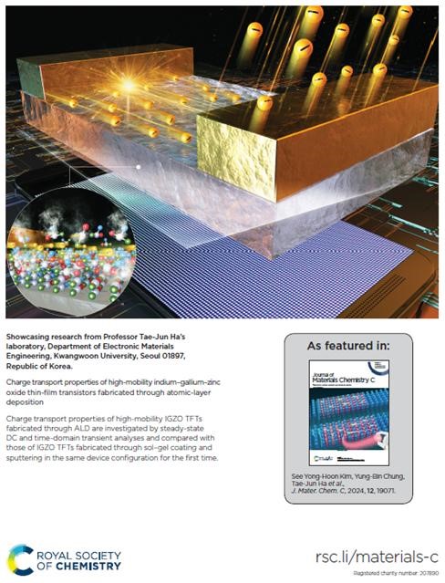
also featured on the Outside Back Cover.
(Reference:
https://doi.org/10.1039/D4TC03560G)
Various methods, such as solution processing,
sputtering, and atomic layer deposition, are being used to deposit IGZO thin
films, the most widely used oxide semiconductor for the channel layer in oxide
thin-film transistors. However, the charge transfer characteristics of IGZO
thin-film transistors fabricated using atomic layer deposition do not align
with conventional analytical models, and comparative studies on the charge
transfer properties of oxide thin-film transistors based on different
deposition methods remain insufficient. In response, Professor Ha Tae-Jun's
research team (Department of Electronic Materials Engineering) conducted a
comparative analysis of the material properties of oxide semiconductor channel
layers based on different deposition methods. Through steady-state DC analysis
and time-domain transient analysis, they successfully and systematically
identified the mechanism behind high-mobility charge transfer characteristics.

Outside Back Cover
published in Journal of Materials Chemistry C
This research, meanwhile, is a result of the
Interactive Display Research Center, where Professor Ha Tae-Jun serves as the
director, as part of the University Innovation Future Challenge project. This
research was carried out with support from the Small and Medium Business
Technology Innovation Development Program, led by the Ministry of SMEs and
Startups, and the Carbon Neutral Industry Core Technology Development Program,
led by the Ministry of Trade, Industry, and Energy. As part of an 8-year
project running from 2023 to 2030 with Samsung Display as the demand-side
company, Professor Ha Tae-Jun's research team is responsible for developing
oxide semiconductor transistor devices and processes.
Professor Ha Tae-Jun's research team is
conducting extensive studies on applying oxide semiconductors to
next-generation display backplanes. Through their work on devices and
processes, the team has published over 60 SCI journal papers and holds more than
30 international and domestic patents. The first author, Park Sang-Jun, a
student in the integrated Master’s and Ph.D. program, joined the IT Development
Team of Samsung Display's Small and Medium-Sized Display Business Unit after
earning his Ph.D. from our university this past August. Meanwhile, Park
Sae-Ryong is actively conducting research on core technologies related to
next-generation semiconductor materials and electronic application devices.